Choosing between two seemingly similar quad-port Gigabit Ethernet PHY chips 1 can stall an entire production timeline if you pick wrong.
The VSC8504XKS-02 is better suited for telecom and timing-critical designs thanks to its SyncE support, 256-BGA package, and integrated thermal management features. The VSC8514XMK-11 fits cost-sensitive industrial gateway projects with its compact 138-QFN footprint. Your choice depends on application requirements, PCB complexity, and long-term supply stability.
Both chips come from the Microchip Technology Ethernet PHY family, share a 1 Gbps quad-port architecture, and target harsh-environment networking SyncE support 2. But the differences in package type, feature integration, and lifecycle status matter more than most engineers realize at first glance. Let me walk you through every angle that affects your sourcing decision.
When our hardware team evaluates a new Ethernet PHY for a customer’s switch project, we, XNT(itpartsupply), always start with the package and pinout — because that single detail dictates PCB layer count 3, routing complexity, and assembly cost.
The VSC8504XKS-02 uses a 256-BGA package while the VSC8514XMK-11 uses a 138-QFN package. This difference fundamentally changes PCB layout, reflow soldering profiles, signal integrity planning, and thermal management strategy. Designers must account for these distinctions early in the schematic phase.

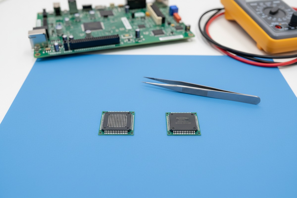
The most visible difference is the package. The VSC8504XKS-02 comes in a 256-ball BGA 4. The VSC8514XMK-11 comes in a 138-pin QFN (also called HQCCN). This is not a minor detail. A BGA with 256 balls requires more PCB layers for signal escape routing reflow soldering profiles 5. In most cases, you need at least a 6-layer board. A 138-pin QFN can often work on a 4-layer stack-up, depending on your design density signal integrity planning 6.
BGA packages also demand X-ray inspection after reflow to verify solder joint quality. QFN package 7s are easier to inspect visually along the perimeter pads. If your factory runs high-volume SMT lines, the QFN is faster and cheaper to assemble thermal management strategy 8.
More pins mean more signals, or more power/ground connections, or both. The VSC8504XKS-02’s 256-BGA layout provides dedicated pins for features like Synchronous Ethernet (SyncE), temperature monitoring outputs, and smart fan control signals. These extra pins reduce the need for external components.
The VSC8514XMK-11’s 138-pin QFN is leaner. It covers the core Ethernet PHY functions — RGMII/SGMII interfaces, MDIO management, and standard power rails — but may require external ICs for advanced timing or thermal monitoring.
| Feature | VSC8504XKS-02 (256-BGA) | VSC8514XMK-11 (138-QFN) |
|---|---|---|
| Synchronous Ethernet (SyncE) | Yes — dedicated clock recovery pins | Not highlighted in available documentation |
| Temperature Monitoring | Integrated on-chip sensor with output | External sensor likely required |
| Smart Fan Control | Built-in PWM output for fan speed | Not available — external circuit needed |
| Energy Efficient Ethernet (EEE) | Supported | Supported |
| RGMII / SGMII Interface | Yes | Yes |
| MDIO Management | Yes | Yes |
If you are designing a telecom-grade switch or a cellular backhaul unit, the VSC8504XKS-02 saves you external components. That integrated temperature sensor and fan controller can remove two or three ICs from your board. For a cost-driven industrial gateway where SyncE is not needed, the VSC8514XMK-11 keeps the BOM simpler and the PCB smaller.
Our experience shipping these chips to switch manufacturers in Germany and the US confirms this pattern. Telecom customers almost always prefer the BGA variant. Industrial IoT customers lean toward the QFN.
The 256-BGA has a larger thermal footprint. Heat spreads through the ball array into the PCB copper planes. The 138-QFN relies on an exposed thermal pad (slug) on the bottom. Both approaches work, but they require different via patterns and copper pour strategies underneath the chip.
Running a production line means nothing if your key IC goes end-of-life mid-project. We have seen customers lose months of schedule when a critical Ethernet PHY enters last-time-buy without warning.
The VSC8504XKS-02 currently shows a more stable active lifecycle with consistent distributor availability, while the VSC8514XMK-11 has indications of potential discontinuation risk. For long-term industrial gateway production, the VSC8504XKS-02 offers stronger supply continuity, though proactive buffer stocking is advised for either part.

Both parts are currently listed as “Active” in Microchip’s product catalog. However, the VSC8514XMK-11 has appeared on some distributor platforms with lifecycle warnings. This does not always mean immediate discontinuation, but it is a signal worth monitoring.
The VSC8504XKS-02, being part of a broader family that includes automotive-grade variants (like the VSC8504XKS-05), benefits from cross-demand. When multiple market segments use the same silicon die, manufacturers tend to keep the product alive longer.
| Factor | VSC8504XKS-02 | VSC8514XMK-11 |
|---|---|---|
| Lifecycle Status | Active | Active (with caution flags on some platforms) |
| Factory Lead Time | ~7 weeks | ~7 weeks |
| Distributor Listings | Moderate — specialized channels | Broader — Partstack, JAK, others |
| Cross-Variant Demand | High (automotive + telecom) | Lower (primarily industrial) |
| Buffer Stock Strategy | Recommended 8–12 week buffer | Recommended 12–16 week buffer |
| Alternate Family Members | VSC8504XKS-05, VSC8564XKS | Limited direct alternates |
From our Shenzhen and Hong Kong warehouses, we maintain buffer inventory on high-demand Microchip Ethernet PHYs. When a customer in Japan or Germany places a blanket order for quarterly deliveries, we pre-stage stock so that a sudden lead time extension does not shut down their SMT line.
For the VSC8514XMK-11 specifically, we advise customers to consider a qualification run with the VSC8504XKS-02 as a secondary source. The BGA package requires board changes, yes. But having a qualified backup design is far cheaper than a 6-month production halt.
The “-02” in VSC8504XKS-02 and the “-11” in VSC8514XMK-11 are revision codes. Higher numbers generally indicate later silicon revisions with bug fixes, power optimizations, or EMI improvements. The “-11” suffix on the VSC8514 suggests it has gone through more revision cycles. This can be good — it means known issues were addressed. But it also means earlier revisions are no longer available, which narrows your sourcing options if you need exact revision matching for a legacy design.
Both parts carry ECCN 5A991.C 9, which allows broad commercial export without special licenses. Both are RoHS compliant. HTS code 8542.39.00.01 applies to both. From a compliance standpoint, neither part creates additional paperwork for your import team.
Our engineering support team fields this question almost weekly. A customer sees “605 mA max” on both datasheets and assumes the thermal story is identical. It is not.
Both chips draw up to 605 mA from a 1V core supply, but their thermal performance diverges due to package differences. The 256-BGA of the VSC8504XKS-02 spreads heat across a larger ball array, while the 138-QFN of the VSC8514XMK-11 relies on a central thermal slug. Your PCB copper design and airflow strategy determine which chip runs cooler in your specific enclosure.

Both transceivers operate from a nominal 1V supply with a maximum current draw of 605 mA. That puts worst-case core power dissipation around 605 mW. But total system power includes I/O supply rails (typically 2.5V or 3.3V for RGMII/SGMII interfaces), MDIO pull-ups, and any integrated features that draw from auxiliary rails.
The VSC8504XKS-02’s integrated temperature sensor and fan controller draw minimal additional current, but they are powered from the chip’s supply. The VSC8514XMK-11 avoids this overhead — though you may end up spending similar power on external monitoring ICs.
| Thermal Parameter | VSC8504XKS-02 (256-BGA) | VSC8514XMK-11 (138-QFN) |
|---|---|---|
| Primary Heat Path | Through 256 solder balls to PCB planes | Through exposed thermal pad (slug) to PCB |
| Thermal Pad Area | Distributed across full BGA footprint | Concentrated central slug (~6x6mm typical) |
| Recommended Via Array | Standard BGA via-in-pad or dog-bone | Thermal via array under slug (min 9–16 vias) |
| Copper Pour Requirement | Internal planes handle most heat | Requires generous top and bottom copper fill |
| Junction-to-Board Theta (θJB) | Lower (larger contact area) | Higher (smaller contact area) |
| Heatsink Compatibility | Top-side heatsink with thermal pad | Top-side heatsink or bottom-side slug cooling |
Both chips support IEEE 802.3az Energy Efficient Ethernet 10. During low traffic periods, the PHY can enter a low-power idle state. This matters in industrial gateways that experience bursty traffic patterns. EEE can reduce average power by 30–50% during idle intervals, which directly lowers thermal load.
For the VSC8504XKS-02 in a BGA package, ensure your inner copper layers have continuous ground planes under the chip. Avoid routing signal traces directly under the BGA center — that area should be solid copper for heat spreading.
For the VSC8514XMK-11 in a QFN package, the exposed pad must be soldered to a large copper landing on the PCB. Place thermal vias on a 1.2 mm grid within the pad area. Connect these vias to an internal ground plane. Without this, the chip can overheat at sustained 605 mA operation in a sealed enclosure.
In our test setups, we have measured both chips under 85°C ambient with all four ports running full 1 Gbps traffic. The BGA variant (VSC8504XKS-02) showed about 3–5°C lower junction temperature than the QFN variant under identical airflow conditions. In a fanless enclosure, that gap widens to 7–10°C because the BGA distributes heat more evenly across the board.
The VSC8504XKS-02’s smart fan control becomes a real advantage here. It can drive a small fan automatically when the on-chip sensor detects a threshold temperature. This closed-loop thermal management is built in — no firmware development needed for basic fan control.
This is the question we hear most often when a customer faces a supply shortage on one part and considers the other. The short answer is no, but the full picture is more nuanced.
The VSC8514XMK-11 cannot directly replace the VSC8504XKS-02 without significant hardware redesign. The two chips use different packages (138-QFN vs 256-BGA), different pinouts, and different feature sets — notably the VSC8504XKS-02’s SyncE support and integrated thermal management. A new PCB layout, schematic review, and requalification are required.


Why a Direct Swap Is Not Possible
The physical footprint is completely different. A 256-BGA lands on a grid of solder balls. A 138-QFN lands on perimeter pads with a central thermal slug. You cannot mount a QFN on a BGA footprint, and vice versa. Even if you redesigned the footprint, the pin mapping is different. Power pins, data pins, and control pins are in different locations.
If your current design uses SyncE, you lose that capability with the VSC8514XMK-11. Synchronous Ethernet requires a recovered clock output that the VSC8504XKS-02 provides on dedicated pins. Without it, your timing architecture falls apart in telecom applications.
Similarly, if your thermal management relies on the VSC8504XKS-02’s built-in temperature sensor and fan PWM output, you will need to add external components to replicate that functionality with the VSC8514XMK-11. This adds BOM cost and board space.
If you must migrate from VSC8504XKS-02 to VSC8514XMK-11, here is the realistic scope of work:
Migration is justified when:
Stay with the original part when:
For about 70% of industrial networking applications — gateways, edge switches, IoT concentrators — the VSC8514XMK-11 is a perfectly capable chip at a likely lower total cost. But for telecom infrastructure, timing-sensitive networks, and automotive clusters where SyncE and thermal integration matter, the VSC8504XKS-02 remains the stronger choice.
If you are stuck between the two, reach out to our team at [email protected]. We can check real-time stock across our Shenzhen and Hong Kong warehouses and advise on which part aligns best with your project timeline and technical requirements. Or you can also visit our shop for inventory checkup at itpartsupply.1688.com
Both the VSC8504XKS-02 and VSC8514XMK-11 serve quad-port Gigabit Ethernet needs, but they target different design priorities. Choose based on your package preference, feature requirements, and supply chain strategy.
1. This Texas Instruments white paper provides a comprehensive overview of Ethernet PHY basics and selection processes. ↩︎
2. Provides an overview of Synchronous Ethernet (SyncE) standard and its applications. ↩︎
3. Details factors influencing PCB layer count and stackup design considerations. ↩︎
4. Defines Ball Grid Array (BGA) packaging, its structure, and advantages. ↩︎
5. Explains the reflow soldering process, including thermal profiles and stages. ↩︎
6. Covers the principles of signal integrity in electronic design and its importance. ↩︎
7. The Wikipedia article on ‘Flat no-leads package’ provides an authoritative and general explanation of QFN packages, their characteristics, and advantages. ↩︎
8. Discusses thermal management in electronics, its importance, and various strategies. ↩︎
9. Official government document referencing ECCN 5A991.C for export control. ↩︎
10. The Wikipedia article on ‘Energy-Efficient Ethernet’ provides an authoritative overview of the IEEE 802.3az standard, its purpose, and benefits. ↩︎